Building Blocks of Creation: The Age of NanoScience and Technology
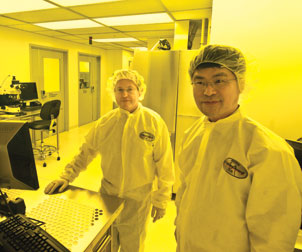 Hrvoje Petek (left) and Hong Koo Kim, codirectors of Pitt’s Petersen Institute for NanoScience and Engineering, are standing in the nanofabrication area of the lab’s “clean room.” The area houses such advanced nanoscale patterning equipment as electron-beam or ion-beam lithography. The process requires an ultraclean environment with a controlled level of air contamination.
 Each year, scientists are making discoveries that advance our understanding of nanoscience, lending substance to the speculation that nanotechnology is a revolutionary force that will profoundly change everything, from the electronics we use to the way doctors practice medicine.
For the most part, the scientists doing the heavy lifting are university-based researchers in physics, chemistry, engineering, biology, and other fields who—given the tools and freedom to explore—are laying the foundation for technologies few thought possible. Prominent among them are the more than 50 University of Pittsburgh researchers who are making significant contributions to the development of nanotechnologies, an endeavor that became a national initiative more than a decade ago.
Today, Pitt researchers are:
• developing special coatings with nanoparticles that prevent surfaces from icing;
• investigating materials containing nanosize bits of semiconductor material to solve one of the chief problems standing in the way of making paint convert sunlight into electricity; and
• integrating biology and nanotechnologies to develop highly sensitive, easy-to-use biosensors that push the boundaries of diagnostic medicine.
These researchers’ exploration of nanoscience has led to homemade devices with remarkable capabilities, including a microscope capable of capturing on film light trapped within metal particles. They’ve set out to discover never-before-seen nanoparticles with properties that could nudge science closer to realizing true quantum computing with the potential for speeds and computational power that would make today’s computers seem snail-like. And Pitt scientists are among the most proactive in assessing the impact these emerging nanotechnologies may have on human health and the environment, as well as in investigating ways to make these technologies safer.
A Matter of Scale
The prefix nano means 10-9, or a billionth. A nanosecond is one billionth of a second; a nanometer, one billionth of a meter. At that scale, the head of a pin seems large, measuring about 2 million nanometers. Nanoscience, therefore, is the study of the world around us at the tiniest of levels. In this field, atoms and molecules are the building blocks for creating new materials and machines. The federal government defines nanoscience as the understanding and control of matter at dimensions between 1 and 100 nanometers; Pitt directs its research towards the smaller, more challenging end of that range, at 1-20 nanometers.
But size is only part of the intrigue, because materials at nanoscale possess remarkably different properties than their larger counterparts. “Very interesting things happen in that range,” says George Klinzing, vice provost for research at Pitt. “If you are looking at friction, it’s different at the level of 1-20 nanometers than it is in large particles of hundreds or thousands of nanometers. The basic laws are different. Understanding that is very important—and challenging. How are you going to manipulate these things? How are you going to make things if you’re not sure how they’ll behave? We put a lot of effort into understanding that.”
The potential impact of nanotechnology on human health, the economy, and national security led President Bill Clinton to establish in 2000 the National Nanotechnology Initiative (NNI) as a multiagency framework to ensure U.S. leadership in the field by investing in basic research to understand nanoscale phenomena and facilitate technology transfer. Since then, NNI funding has risen approximately fourfold, from $462 million to nearly $1.8 billion in fiscal year 2010.
Pitt’s traditional strength in materials research meant that, even before NNI, University researchers in fields ranging from chemistry to physics were investigating nanoscience with the support of a growing number of federal agencies eager to develop the new technology. In December 2002, under the leadership of then-Provost James V. Maher, Pitt created the Institute for NanoScience and Engineering to support and integrate the work of the increasing number of faculty from diverse disciplines embarking on nanoscience research.
Within four years, the institute was renamed the Petersen Institute for NanoScience and Engineering (PINSE). The institute’s Benedum Hall home was renovated to accommodate a state-of-the-art nanoscale fabrication and characterization facility, the range of sophisticated instruments available to researches expanded significantly, and, with a $5 million gift from the Petersens, an endowment was created to support the work of Pitt’s scientists.
An Uncommon Resource
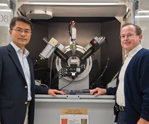 One of the key instruments in Pitt’s nano lab is the X-ray diffraction system, which analyzes the structural properties of nanomaterials at the atomic or molecular level. The University’s Petersen Institute for NanoScience and Engineering (PINSE) has invested almost $12 million to stock its facility with more than two dozen of the most advanced instruments required for high-level nanoscience research. Pictured are Hong Koo Kim (left) and Hrvoje Petek.
Today PINSE stands as one of the most up-to-date, comprehensive institutes for nanoscale research on a university campus, offering scientists an uncommon asset for doing science at nanoscale and for securing external support for their work.
Few universities provide facilities and instruments to both characterize and fabricate nanomaterials in one place. “From the beginning, our philosophy has been understanding nanomaterials through characterization and doing manipulation, fabrication, and synthesis into a designed structure in a synergistic environment,” says Pitt’s Hong Koo Kim, the Bell of Pennsylvania/Bell Atlantic Professor of Electrical and Computer Engineering and codirector of PINSE. “Many other research facilities focus on either characterization or fabrication, but when you emphasize only one, you may miss important aspects of the other and cannot develop a holistic picture.”
The sophistication of the instruments available to scientists has done much to advance their understanding of nanomaterials and structures. PINSE has invested nearly $12 million to stock its characterization and fabrication facility with more than two dozen of the most advanced instruments required for high-level nanoscience research demands. All are housed in a clean-room environment. An example of an instrument available for characterization is the transmission electron microscope, which has a resolution of less than one nanometer. It allows scientists to visualize the atomic arrangement of nanomaterial and reconstruct the way atoms are arranged. On the fabrication side, Pitt scientists have access to instruments such as electron beam and focused ion beam nanolithography systems, which enable the researchers to build almost anything at nanoscale to their precise design specifications.
PINSE employs three technical staff members, a manager, and two research associates and provides resources and support to more than 50 affiliated faculty researchers across several disciplines.
In 2009, PINSE opened its doors to researchers beyond the Pitt campus, including individuals in industry and at other academic institutions. About a half-dozen PINSE-affiliated faculty also are engaged in collaborative research projects with various companies, and the list is expected to grow as the University steps up efforts to form industry partnerships around nanotechnology.
PINSE-affiliated faculty also are developing undergraduate and graduate-level coursework in nanoscience and nanotechnology, including entry-level courses in electrical engineering and a laboratory course that allows undergraduates to experience working with the leading-edge instruments and other amenities in the characterization and fabrication facility. “The philosophy is not only to educate our students in theory, but also to give them hands-on experience as well, because we see more and more job openings in the emerging nanotechnology industry,” says Kim.
Recognition at the Highest Levels
Nanotechnology research at Pitt is showing significant potential for helping to develop the kind of longer-term industry relationships the University seeks. That is the result of several factors, including the expertise of faculty members, the breadth of that expertise and their experience, and the expanding list of their accomplishments.
PINSE-affiliated faculty are involved in more than 100 nanoscience-related research projects during any given year. Their work is supported by an estimated $12 million in grants from federal government agencies, ranging from the National Science Foundation (NSF) and the Department of Energy to the Department of Defense and the National Institute of Standards and Technology. Many faculty have received prestigious awards, including at least 10 PINSE-affiliated scientists who have earned an NSF Career Award.
In fact, Pitt is regularly ranked among the top seven universities in both nanotechnology research and nanotechnology commercialization by Small Times, the leading nanotechnology trade publication. “Its breadth of expertise, resources, and publishing activities,” the magazine recently wrote, “puts Pitt near the top for micro and nanotech research.”
A Quantum Challenge
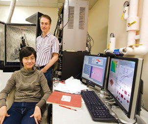 Jeremy Levy, a professor of physics and astronomy in Pitt’s School of Arts and Sciences, researches nanosize structures and hopes to advance the basic science that underlies quantum computing. He and Cheng Cen, who recently earned her PhD in Levy’s lab, are in front of an atomic-force microscope that is used to create the nanosize structures.
 For decades, quantum computing has been a grand challenge for physicists seeking to realize nanoscience’s potential for surpassing the speeds and computational abilities of today’s best computers. Jeremy Levy’s ambitious experimental research program is directly addressing the many challenges that must be overcome to reach that elusive goal.
Levy, a professor of physics and astronomy in Pitt’s School of Arts and Sciences and director of the Center for Oxide-Semiconductor Materials for Quantum Computation, works to understand and create nanosize structures, investigate their properties, and discover new physics in the process. His laboratory specializes in a class of materials known as complex oxides, which act somewhat like semiconductors but have a more robust behavior.
Working with a system consisting of two oxides—a layer of lanthanum aluminate about 1 nanometer thick grown onto strontium titanate—Levy found that the interface between the two materials can be switched between a conducting phase and an insulating phase. His lab also invented a method to control the process, which, he says, is reminiscent of an Etch A Sketch® toy. From those oxide nanostructures, his lab was able to make a transistor roughly 1,000 times smaller than those used in today’s computers.
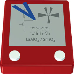 Jeremy Levy, Pitt professor of physics and astronomy, invented a way to control the way in which electricity flows at the interface between two types of oxides. Using this process, which he likens to an Etch A Sketch® toy, Levy made a transistor about 1,000 times smaller than those in today’s computers.
His work with oxide nanostructures has implications for advancing the basic science that underlies quantum computing. Recently, he was awarded a $7.5 million Multidisciplinary University Research Initiative grant from the U.S. Air Force Office of Scientific Research to support his work on quantum preservation, simulation, and transfer in oxide nanostructures. “What we are trying to do is to develop new types of quantum technology that utilize the properties of superconductors,” says Levy. In one of those projects, researchers in Levy’s lab are trying to discover new particles that have been predicted but never observed before in the universe. These particles possess topological properties that allow them to be “braided” in ways that offer advantages for developing a quantum computer, such as making it more tolerant of errors. “We are dealing with some of the most challenging parts of quantum computing,” Levy says.
Back to the Future
When it comes to nanomachines, none have been around longer than a prolific and diverse population of viruses known as bacteriophages. Recent evidence suggests these microorganisms evolved in nature at least 3.5 billion years ago, perhaps near the beginning of life itself—the “original nanomachines,” Roger Hendrix calls them.
One notable attribute of bacteriophages is their ability to infect bacteria. They can penetrate bacterial cells, become one with them, and either kill or alter them. But they are not well understood, despite their advanced age and the fact that some 10 million trillion trillion individual bacteriophages are estimated to be roaming the planet at any one time.
A Distinguished Professor of Biological Sciences in Pitt’s School of Arts and Sciences, Hendrix studies how bacteriophages—which have been refined by natural selection over billions of years of existence—are assembled from their component parts. Each bacteriophage has a protein shell for a head and a tail that is part of the machinery for injecting DNA into the cell that it infects.
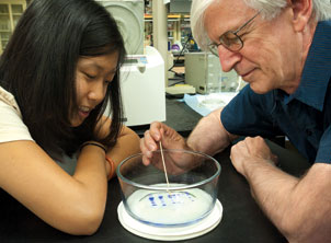 Roger Hendrix, Distinguished Professor of Biological Sciences in Pitt’s School of Arts and Sciences, studies bacteriophages, which are viruses that evolved at least 3.5 billion years ago. Here, Hendrix works with Bonnie La, a second-year doctoral student, as they perform an electrophoretic analysis of the proteins of one of the phages studied in Hendrix’s lab.
Of particular interest to Hendrix is the introduction of DNA during the head assembly process and the elaborate rearrangement the protein shell then undergoes to make it more stable, sturdy, and resistant. The tail assembly also has its mysteries to solve. One is understanding how the tail is assembled to the same length for all bacteriophages in a population.
“It’s a general question about how you assemble biological structures or nanostructures,” says Hendrix. “How are the dimensions determined? If you’re making a structure out of identical bricks, how do you know when to stop piling up the bricks?”
Answering such questions about bacteriophage assembly could have implications for the development of a range of nanotechnologies. “These nanomachines are more sophisticated than anything anyone can build in the lab these days,” says Hendrix. “So understanding how they work is informative for understanding how we can make nanomachines.”
Breaking Speed Limits
A modern computer processor with a clock rate of a few gigahertzes can operate its transistors at a rate of about once every nanosecond. Most people would likely see that as fast; Hrvoje Petek sees it as an opportunity.
“In principle,” says Petek, a physics and a chemistry professor in Pitt’s School of Arts and Sciences and PINSE’s codirector, “we should be able to make electronic devices that are much faster and that would consume much less energy if we could combine light with conventional electronics.”
The focus of Petek’s research is ultrafast phenomena in solid-state materials. And by ultrafast, he means phenomena that occur on time scales that are less than 10-12 second. An area of particular interest is ultrafast electron microscopy. One result of this work is the time-resolved photoemission electron microscope his laboratory developed that can image electric fields in a solid-state material or nanostructures with a remarkable 10-14 second time resolution.
“We have speeded up microscopy by many orders of magnitude,” says Petek. “What this allows us to do is to image light on a nanometer scale.”
Using the microscope, Petek is able to make movies of light being trapped inside metal particles and metal films. “The light pulses we can trap in nanofilms on nanometer scale may be combined with conventional electronic devices to speed them up and to reduce their energy consumption. To achieve that, the first thing that is necessary is to take movies of these trapped light pulses inside a metal film on both a femtosecond (one quadrillionth of a second) temporal scale and a nanometer spatial scale.”
Petek is also exploring single-molecule machines. Using a scanning tunneling microscope, for example, he can shoot single electrons into a molecule and learn how its internal structure can be manipulated. It’s a step into the next frontier in electronics. “There is going to be a limit on how far conventional electronic devices can be shrunk,” Petek says. “At some point, rather than using silicon, there may be advantages to using molecular materials. Such single-molecule devices represent the smallest miniaturization of a device one can imagine.”
Ice and Sun
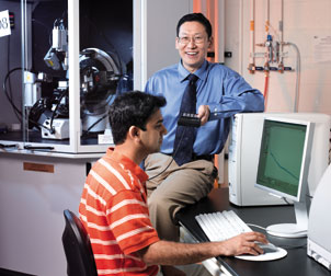 Part of the nanoscience research being done by Di Gao, a Pitt assistant professor of chemical and petroleum engineering and a W. K. Whiteford Faculty Fellow, is discovering how nanoparticles can be used to prevent ice buildup on road surfaces as well as on airplane wings and power lines. Here, Gao works with Ashish Yeri, a fourth-year PhD student. The large machine in the background is an X-ray diffractometer, which is used to examine the crystallinity of materials.
 In his laboratory, Di Gao is investigating ways of modifying surfaces with nanoparticles that some day might lead to ice-proof roads, while also exploring the use of nanowire arrays to solve a stubborn problem confounding the development of a promising new technology for harnessing the power of the sun.
Gao is applying his study of superhydrophobic surfaces to develop coatings that prevent the conditions necessary for icing to begin. Particle size, in particular, is critical. And if making an anti-icing material is the goal, smaller is better. Gao’s laboratory exploits that scientific fact by developing coatings that are a blend of polymers and nanoparticles small enough to deny supercooled water the nucleation center necessary for ice to form.
“Water basically gets bounced away,” says Gao, an assistant professor of chemical and petroleum engineering and a William Kepler Whiteford Faculty Fellow at Pitt. “Eventually this can be applied to power lines and the wings of airplanes to prevent icing.”
Road surfaces present another challenge. The coating when applied to a road surface won’t endure the abuse of traffic and other factors. So, Gao is collaborating with other Pitt scientists to make an anti-icing concrete containing nanoparticles.
Gao’s laboratory is also focusing its expertise on improving the efficiency of dye-sensitized solar cells, an emerging technology with the potential to harvest energy at a significantly lower cost than silicon-based cells; this research is attracting considerable attention throughout the world.
The emerging technology’s potential won’t be realized, however, until these new solar cells can be made to do a better job converting infrared light into electricity. One problem with current dye-sensitive solar cells is their disordered nanoparticle network, which requires electrons to hop between particles. Gao is trying to solve that problem by using ordered, or vertically aligned, titanium oxide nanowire arrays, which, he says, “give the electrons a freeway to get out of the cell and improve the electron transport efficiency of the anode.”
Unconventional Optics
A basic premise of conventional optics is that light bends in a certain way when it enters a different medium. PINSE codirector Kim is interested in manipulating light in novel ways that cannot be achieved with conventional optics.
One of his interests in particular is making light bend the opposite way from its natural way of bending— and developing new nanomaterials that will allow that to be exploited as a platform for new applications ranging from extremely high resolution imaging to advanced photovoltaic devices.
While the potential for so-called negative-index metamaterials has been recognized and pursued for several years, moving the technology from the laboratory to real-world applications has been problematic. In most approaches, for example, light is lost as it travels through the metamaterials. And these materials work only for a narrow spectral range. Both drawbacks limit the materials’ practical usefulness.
Kim, however, is taking a different approach, developing a nano-optic structure that can bend light in a negative direction in a way that is amenable to a wide range of wavelengths, is relatively easy to fabricate, and is almost lossless, meaning that light passes through it with minimal loss of energy. Such properties open the door to a host of possible advanced uses.
For instance, the new nano-optic structure, when used for imaging, could make it possible to produce smaller transistor patterns. The structure also has promise as an advanced lens capable of observing extremely small objects, achieving higher-resolution imaging than is currently available.
It could also lead to enhancing efficiencies of photovoltaic devices. “By bending light, this approach, this structure, allows the light to interact with thin-film solar cell material at longer distances,” says Kim. “That means better absorption and better utilization of that solar energy, which produces higher efficiencies in electricity generation.”
Photovoltaic Paint
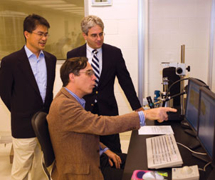 Pitt’s David Waldeck (seated) works with Hong Koo Kim (standing left), and David Geller, the Richard L. Simmons Professor of Surgery in Pitt’s School of Medicine and codirector of the UPMC Liver Cancer Center. Waldeck’s research is focused on finding a way to use nanoparticles to make a commercially viable photovoltaic paint that can convert sunlight into electricity. Waldeck is a professor of chemistry and chair of the Department of Chemistry in the School of Arts and Sciences.
Among the potential benefits of nanoparticles is the possibility of finally solving one of the major problems standing in the way of realizing a commercially viable photovoltaic paint able to convert sunlight into electricity. Although the world is moving closer to such a solar-power paint, available technologies fall short of reaching the needed conversion efficiencies because too few of the solar photons they absorb are converted into electrons. One scientist working on that problem is David Waldeck, a professor of chemistry and chair in Pitt’s Department of Chemistry in the School of Arts and Sciences, whose research interests include understanding and controlling electron motion on nanometer scales.
Waldeck’s laboratory is making composite materials of nanoscale bits of semiconductor that are mixed with a conducting polymer material. These semiconductor nanoparticles have several advantages. “We are able to tune the color of light they absorb and where their energy levels lie by changing their size,” says Waldeck. “By changing the surface coating on the nanoparticles, we can place them at the interface of two different polymers and absorb most of the light at the boundary of the polymers. Because we can make one of the polymers be a cathode and the other polymer an anode— like the poles of a battery— absorbing the light at that boundary allows us to very efficiently drive the electron from one phase to another.”
Such a development would offer a more efficient and less expensive process for converting light into electricity. “If it all works, you will be able to ‘paint’ your roof one day, plug it in, and save on your electricity bill. That’s the basic idea.”
Another research interest of Waldeck’s is understanding how to manipulate light on nanometer-length scales. This work has led to a collaborative project with Joanne Yeh, a professor in the Pitt School of Medicine’s Department of Structural Biology, to develop enhanced biosensors that have drawn support from the National Institutes of Health and the National Aeronautics and Space Administration.
Waldeck’s laboratory is creating thin metal films approximately 200 nanometers thick that are structured with holes, rings, or slits that enable them to direct the path along which light travels. Yeh’s laboratory integrates biological materials onto these nanoplasmonic devices. The idea is to create new nanoplatforms for performing chemical and biological analysis using the same concepts of miniaturization and integration that have been so successfully applied to electronics.
A Role in Human Health
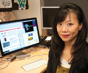 In the laboratory of Joanne Yeh, a professor in the School of Medicine’s Department of Structural Biology, researchers are working on applying nanotechnology to medical problems. Yeh’s lab has, for example, developed a biosensor capable of detecting prostate-specific antigen (PSA) levels in blood and urine. Currently, a blood test is the most common means of measuring elevated PSA levels, which can indicate cancer or other prostate problems. Yeh’s computer screen shows images of what her lab’s nanobiosensors look like at the atomic or nanoscale.
 Applying nanotechnology to clinically relevant medical problems is an area attracting a great deal of interest and one that Pitt researchers have actively explored for several years.
Yeh, for example, has developed in her laboratory a novel approach called “coordinated biosensing” to make highly sensitive, biodegradable sensors for early detection of diseases. This process involves integrating another area of study in Yeh’s laboratory, elucidation of the three-dimensional atomic resolution structures of proteins and nucleic acids by the single crystal X-ray diffraction method to form active “nanobioassemblies.” Her approach enables the precise spatial incorporation of each sensor component to maximize the functionality and sensitivity of the biosensor. In addition to being highly sensitive, these biosensors are platform-independent and easily miniaturized.
Using this approach, Yeh’s lab developed a biosensor capable of detecting prostate-specific antigen (PSA) with unprecedented sensitivities. Elevated PSA levels in men are an indication of prostate cancer and other prostate disorders. A blood test administered in a doctor’s office or clinic is currently the most common method of measuring PSA levels. Yeh’s biosensor has the potential to change that. One clear advantage Yeh’s biosensor holds over conventional tests is that it accurately detects PSA in urine as well as in serum.
“We’ve tested our biosensors, and they are very accurate and robust,” says Yeh. Moreover, they are small, inexpensive, and easy to use. The idea is that this technology will someday become a self-administered sensor that can be purchased at a pharmacy, much like today’s home pregnancy tests. The sensors also have the potential to improve early detection of prostate cancer in places where health care resources are limited, like rural regions and Third World nations.
Yeh says the PSA biosensor is a preview of what is likely to develop from the marriage of nanotechnology and biomedicine. “Our goal is to develop these nanobiosensors not only for PSA [tests] but also for other diseases or other clinical markers that are relevant for determining abnormal disease states.”
Supersensitive Detectors
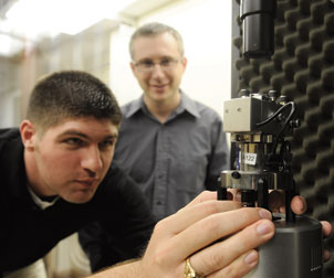 Alexander Star (background), an assistant professor of chemistry in Pitt's School of Arts & Sciences, is working with other researchers in his lab to turn nanotubes into chemical and biological sensors. His research group recently used tubes with diameters 100,000 times smaller than a human hair to develop a sensor that can warn asthma sufferers of an impending attack. Here, Brett Allen, who recently completed his doctoral degree in chemistry under Star’s supervision, uses an atomic force microscope to visualize carbon nanotubes.
Turning carbon nanotubes into chemical and biological sensors is one of Alexander Star’s research interests. His research group recently used tubes with diameters 100,000 times smaller than a human hair to develop a sensor that can warn asthma sufferers of an impending attack.
The sensor detects concentrations of nitric oxide in human breath. Nitric oxide is a marker of inflammation. Rising levels of the gas suggest a buildup of inflammation in the airways, which can predict an asthma attack.
A nanotube’s advantage in detection is its extremely small size. When gas molecules like nitric oxide bind to the surface, they significantly impede the flow of electrical current— an event that can be detected. “Ideally, such sensors could be sold in pharmacies, like glucose sensors that test glucose levels in blood,” says Star, an assistant professor of chemistry at Pitt. “People would be able to detect the nitric oxide levels in their breath and take their asthma medication as a preventive treatment.”
Star’s lab also found that cup-like nanomaterials can be built with nitrogen by stopping their growth at small segments. The lab is investigating how these nanocups can be joined to form hollow capsules, which might someday be used for targeted drug delivery. “We can figure out how to fill them with drugs and hopefully use them as next-generation therapeutic systems,” Star adds.
For that to happen, nanomaterials must be made to safely degrade in the human body. Star’s research includes investigating the impact such materials have on the environment and on human cells. His lab, for example, was the first to discover that enzymes derived from horseradish could be used as a catalyst for degrading nanotubes.
Recently, the first human enzyme capable of biodegrading carbon nanotubes was identified by an international team of researchers led by Valerian Kagan, a professor and vice chair in the Department of Environmental and Occupational Health in Pitt’s Graduate School of Public Health. Tests on mice have suggested that inhaling carbon nanotubes can result in severe inflammation in the lungs and early onset of fibrosis. The researchers found that nanotubes degraded with the human enzyme myeloperoxidase did not cause lung inflammation.
The findings suggest that carbon nanotubes might someday be developed as a safe method of delivering drugs and that a natural treatment for people exposed to carbon nanotubes is possible.
Pitt researchers, in fact, have been among the most proactive in investigating the potential adverse effects of nanotechnology. “Carbon nanotubes are being used in products, and companies want to produce them in large quantities,” says Star, who was among the researchers involved in the Kagan study. “It’s only appropriate to look at how they affect the body and the environment.”
Far-Reaching Contributions
In microelectronics, basic research in solid-state physics and semiconductor materials led to new circuitry, small-scale chips, and other advances from which powerful personal computers, cell phones, and other technologies widely used today have evolved. The NNI, more than a decade ago, envisioned nanotechnology taking a similar trajectory, starting with understanding the underlying science and creating simple materials before evolving to more advanced materials and structures.
“Good research has specific goals,” says Vice Provost Klinzing. “Often the goal is to answer an important question, improve an existing technology, or create a transformational technology. The importance of these goals is in proportion to their capacity to help improve the quality of our lives, reduce suffering, and lift the human spirit.”
Pitt nanoscience investigators, accepting those challenges, are well positioned to make more than incremental advances. “We anticipate making more fundamental contributions in the future that will be even more far-reaching,” says Kim.
Other Stories From This Issue
On the Freedom Road

Follow a group of Pitt students on the Returning to the Roots of Civil Rights bus tour, a nine-day, 2,300-mile journey crisscrossing five states.
Day 1: The Awakening
Day 2: Deep Impressions
Day 3: Music, Montgomery, and More
Day 4: Looking Back, Looking Forward
Day 5: Learning to Remember
Day 6: The Mountaintop
Day 7: Slavery and Beyond
Day 8: Lessons to Bring Home
Day 9: Final Lessons

